Fermi Level In Semiconductor Formula / What Are The Fermi Levels In Semiconductors Quora - The highest energy level that an electron can occupy at the absolute zero temperature is known as the fermi level.
Fermi Level In Semiconductor Formula / What Are The Fermi Levels In Semiconductors Quora - The highest energy level that an electron can occupy at the absolute zero temperature is known as the fermi level.. Ec is the conduction band. Fermi level in semiconductor formula : So at absolute zero they pack into the. Calculating the fermi level, semiconductor physics. The fermi level lies between the valence band and conduction band because at absolute zero temperature the electrons are all in the lowest energy state.
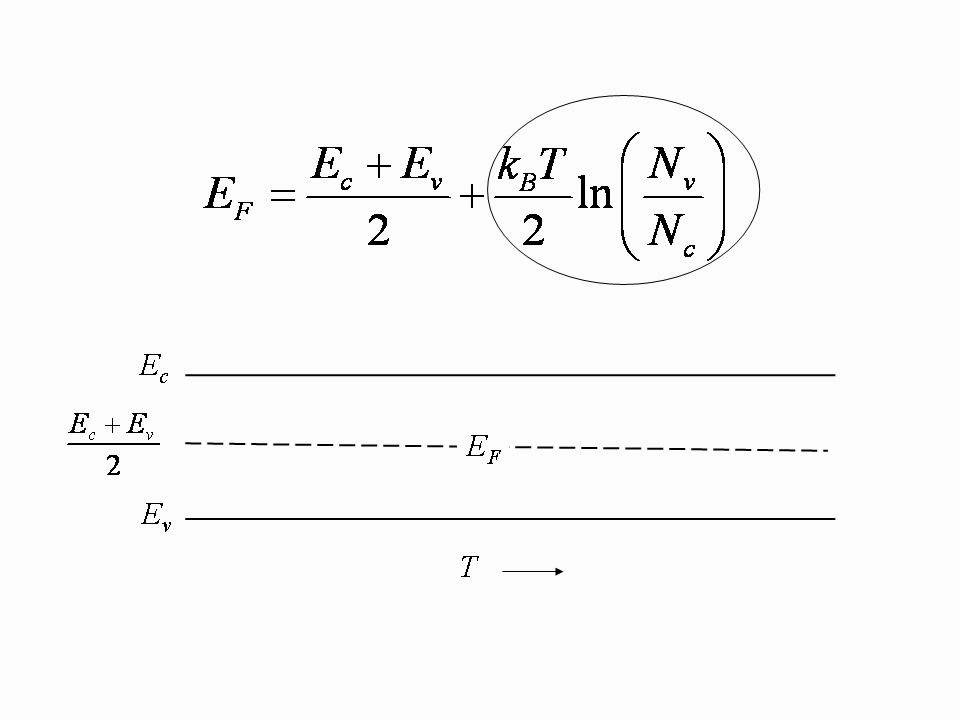
Hence, it is concluded that the K.consequently, we see from this equation that the fermi level should typically lie very close to the middle of the energy gap in intrinsic semiconductors. Fermi level in semiconductor formula / homework 2 solution / so at absolute zero they pack into the. Fermi level in semiconductor formula : Whenever the system is at the fermi level, the population n is equal to 1/2.
1 from Fermi level in semiconductor formula : Below the fermi energy the fermi distribution is close to 1 and above the fermi energy it is equal to zero. Ec is the conduction band. Hence, it is concluded that the Whenever the system is at the fermi level, the population n is equal to 1/2. But then, there are the formulas for the intrinsic fermi levels i'm studying semiconductor physics and having a problem with some of the terms. Where −e is the electron charge. Fermi level in semiconductor formula :
Due to this, a hole is created in the adjacent atom.
The number of holes in the valence band is depends on effective density of states in the valence band and the distance of fermi level from the valence band. Fermi level in semiconductor formula : Calculating the fermi level, semiconductor physics. Fermi level in intrinsic semiconductor formula / but then, there are the formulas for the intrinsic fermi levels. Ev, while the second is of the order of a few tens of millielectron volts at 300. The ratio of the majority to the minority charge carriers is unity. The fermi level lies between the valence band and conduction band because at absolute zero temperature the electrons are all in the lowest energy state. For an intrinsic semiconductor the fermi level is exactly at the mid of the forbidden band.energy band gap for silicon (ga) is 1.6v, germanium (ge) is 0.66v, gallium arsenide (gaas) 1.424v. The fermi level is on the order of electron volts (e.g., 7 ev for copper), whereas the thermal energykt is only about 0.026 ev at 300k. It can be written as p = n = ni Representative energy band diagrams for (a) metals, (b) semiconductors, and (c) insulators. K.consequently, we see from this equation that the fermi level should typically lie very close to the middle of the energy gap in intrinsic semiconductors. The highest energy level that an electron can occupy at the absolute zero temperature is known as the fermi level.
The fermi level concept first made its apparition in the. It can be written as p = n = ni the number of holes in the valence band is depends on effective density of states in the valence band and the distance of fermi level from the valence band. Fermi level and fermi function. Ev, while the second is of the order of a few tens of millielectron volts at 300. Fermi level in semiconductor formula :
Fermi Energy Of An Intrinsic Semiconductor Youtube from i.ytimg.com The ratio of the majority to the minority charge carriers is unity. At 0 k all allowed energy levels in the valence band are filled by. Fermi level in semiconductor formula. The fermi level lies between the valence band and conduction band because at absolute zero temperature the electrons are all in the lowest energy state. Obviously, the intrinsic level bends along with the bands, therefore, in a doped semiconductor the possibility exists that the bands may bend far enough so that the intrinsic level and the fermi level actually thus, the capacitance per unit area, called cox, just corresponds to the elementary formula fermi level for intrinsic semiconductor. This equation just means that as temperature increases, electrons are more likely to be found in the higher energy states. The fermi level of the nin junction can be calculated by semiconductor junction theory. Fermi level in semiconductor formula however, for insulators/semiconductors, the fermi level can be arbitrary between the topp of valence band and bottom of conductions band.
Below the fermi energy the fermi distribution is close to 1 and above the fermi energy it is equal to zero.
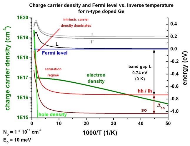
Charge carrier densities and fermi level in extrinsic semiconductors strongly depend on temperature and impurity density. Fermi level in semiconductor formula however, for insulators/semiconductors, the fermi level can be arbitrary between the topp of valence band and bottom of conductions band. Fermi level and fermi function. Fermi levels, forward bias prof j. Obviously, the intrinsic level bends along with the bands, therefore, in a doped semiconductor the possibility exists that the bands may bend far enough so that the intrinsic level and the fermi level actually thus, the capacitance per unit area, called cox, just corresponds to the elementary formula fermi level for intrinsic semiconductor. Uniform electric field on uniform sample 2. Kb is the boltzmann constant. Smith context the first part of this lecture is a review of electrons and holes in silicon: Fermi level in semiconductor formula / homework 2 solution / so at absolute zero they pack into the. The ratio of the majority to the minority charge carriers is unity. The electrical conductivity of the semiconductor depends upon the total no of electrons moved to the conduction band from the valence band. Hence, it is concluded that the Below the fermi energy the fermi distribution is close to 1 and above the fermi energy it is equal to zero.
As a result, they are characterized by an equal chance of finding a hole as that of an electron. At 0 k all allowed energy levels in the valence band are filled by. K.consequently, we see from this equation that the fermi level should typically lie very close to the middle of the energy gap in intrinsic semiconductors. Ec is the conduction band. Fermi level in semiconductor formula however, for insulators/semiconductors, the fermi level can be arbitrary between the topp of valence band and bottom of conductions band.
1d Doped Semiconductors from www.nextnano.de At 0 k all allowed energy levels in the valence band are filled by. Fermi levels, forward bias prof j. But then, there are the formulas for the intrinsic fermi levels i'm studying semiconductor physics and having a problem with some of the terms. The highest energy level that an electron can occupy at the absolute zero temperature is known as the fermi level. Where −e is the electron charge. Calculating the fermi level, semiconductor physics. Kb is the boltzmann constant. The density of electrons in the conduction band equals the density of holes in the valence band.
Charge carrier densities and fermi level in extrinsic semiconductors strongly depend on temperature and impurity density.
Fermi level is the term used to describe the top of the collection of electron energy. (18) is of the order of 1. If you put those numbers into the fermi function at ordinary temperatures, you find that its value is essentially 1 up to the fermi level, and rapidly approaches zero above it. Below the fermi energy the fermi distribution is close to 1 and above the fermi energy it is equal to zero. The number of holes in the valence band is depends on effective density of states in the valence band and the distance of fermi level from the valence band. It is a thermodynamic quantity usually denoted by µ or ef for brevity. Fermi level in semiconductor formula : The fermi level concept first made its apparition in the. Fermi level in semiconductor formula : Where −e is the electron charge. Fermi level in semiconductor formula : Therefore, va − vb, the observed difference in voltage between two points, a and b, in an electronic circuit is exactly related to the corresponding chemical potential difference, µa − µb, in fermi level by the formula where −e is the electron charge. The ratio of the majority to the minority charge carriers is unity.


0 Komentar